


Write Protection
1. Introduction
本ドキュメントは、シリアルフラッシュメモリーのライトプロテクション機能について記述するものです。 本ドキュメントでは、W25Q16DV 製品(Rev. G 参照)をベースに機能の説明をしますが、最終的にはご使用になる製品データシートにてプロテクト領域やプロテクトに使用するステータスビットの確認をお願いしま す。
This document describes the write protection function of serial flash memory. In this document, functions are described based on the W25Q16DV product (see Rev. G), but in the end, please confirm the status bits used for the protection area and protection in the product data sheet to be used.
2. Explanation of /WP pin function
シリアルフラッシュメモリーには、ハードウェア端子として/WP 端子があります。(下記端子配列を参照願います。)
The serial flash memory has / WP terminal as hardware terminal. (Please refer to the following pin configuration.)
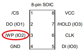
Note: /WP=Write Protect Input
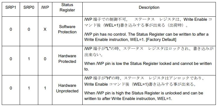
/WP 端子は、メモリーアレイ領域に対するプロテクト機能ではありません。 シリアルフラッシュメモリーのステータス レジスタ ビットSRP[1:0]と/WP 端子の状態にてステータス レジスタへの書き込みをプロテクト/アンプロテクトする機能になります。
The / WP pin is not a protection function for the memory array area. It is a function to protect/unprotect the writing to the status register according to the status of the status register bit SRP [1: 0] and / WP pin of serial flash memory.
7.1.7 Status Register Protect (SRP1, SRP0)
3. Explanation of Memory Array Protection Method
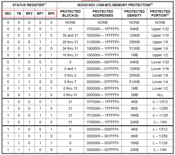
ここでは、メモリーアレイ領域に対するプロテクの方法について記述します。 メモリーアレイ領域への書き込みをプロテクトするには、ステータス レジスタのBlock Protect Bits BP[2:0] ビットを使用してプロテクトを設定します。 初期状態(出荷時)は、”0”(プロテクトされていません)。 メモリーアレイ領域のプロテクに関するステータス レジスタ ビットは、他に SEC, TB, CMP ビットがあります。7.1.11 status Register Memory Protection [データシート 17 ページ以降]にて各ビットの状態によりどの領域がプロテクトされるか表になっています。 下記にデータシートからの一部抜粋を示します。
This section describes how to protect memory array areas. To protect writes to the memory array area, use the Block Protect Bits BP [2: 0] bits in the status register to set protection. The initial state (factory default) is “0” (not protected). Other status register bits related to memory array area protection are SEC, TB and CMP bits. 7.1.11 status Register Memory Protection [Data sheet page 17 and later] shows which area is protected depending on the status of each bit. Below is a partial excerpt from the data sheet.
7.1.11 Status Register Memory Protection (CMP=0)
4. Status Register
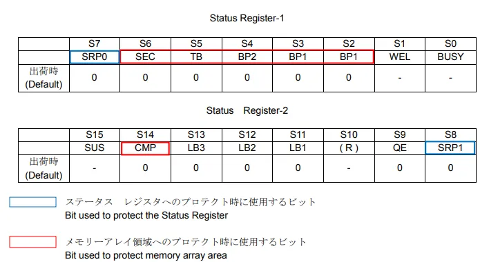
シリアルフラッシュメモリーには、以下のステータス レジスタが用意されています。 本ドキュメントの説明に出てくるビットです。
The serial flash memory has the following status registers. It is a bit that appears in the explanation of this document.
上記ステータス レジスタへの書き込みは、以下のコマンドを使用して変更を行います。
◆ 不揮発性領域のステータス レジスタ ビットへの書き込み
Write Enable (06h) + Write Status Register (01h)
◆ 揮発性領域のステータス レジスタ ビットへの書き込み
Write Enable for Volatile Status Register (50h) + Write Status Register (01h)
注)電源オフにて揮発性のステータス レジスタ ビットの値は失われ、次回電源オン時には不揮発性のステータスレジスタ ビットの値が再ロードされます。
以下の事より、頻繁にプロテクト状態を変更されるようなシステムにおきましては、不揮発性領域のステータス レジスタ ビットをプロテクトに設定し起動し、稼働中は揮発性領域のステータス レジスタ ビットによる変更を推奨致します。
設定変更時間の短縮 不揮発性ビット(10ms) vs 揮発性ビット(50ns)
書き換え回数の低減(メモリーセルアレイ同様に書き換え回数が 100K のため)
To write to the above Status Register, use the following command to make change.
◆ Write to the Status Register bit of the non-volatile area
Write Enable (06h) + Write Status Register (01h)
◆ Write to the Status Register bit of the volatile area
Write Enable for Volatile Status Register (50h) + Write Status Register (01h)
Note: The value of volatile Status Register bit is lost at power off, and the value of non-volatile status register bits are reloaded at next power on.
From the following, in a system where the protection status is frequently changed, the status register bit of non-volatile area is set to protection and power-on, and it is recommended to change the status register bit of volatile area during operation.
Reduced configuration change time Non-volatile bit (10ms) vs Volatile bit (50ns)
Reduction in the number of rewrites (because the number of rewrite is 100K as well as the memory cell array)
5. Another Write Protect method using Individual Block Locks
W25Q-JV シリーズ及び W25Q-FW/JW シリーズにて Individual Block Locks を使用して別のプロテクト方法を提供しています。 ステータス レジスタ 3(下記では 256Mb の例)にある WPS ビットを使用してメモリーアレイ領域のプロテクト方法を決定します。
In the W25Q-JV series and W25Q-FW / JW series, we offer another protection method using Individual Block Locks. Use the WPS bit in Status Register 3 (below is an example of 256Mb) to determine how to protect the memory array area.
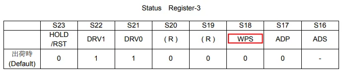
WPS=0: CMP, TB, BP[3:0]ビットを使用してメモリーアレイの特定の領域をプロテクトします。
Use CMP, TB, BP[3:0] bits to protect specific area of memory array.
WPS=1: プロテクトのために個別ブロックロックを利用します。
Use Individual Block Lock for protection.
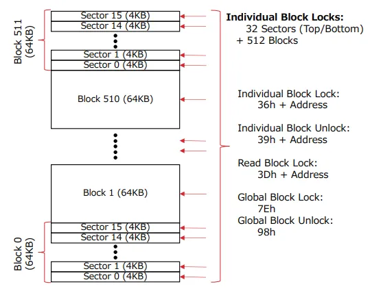
下記に 256Mb の場合のIndividual Block/Sector Locks を示します。各 64KB ブロック(上部と下部のブロックを除く合計 510 ブロック)および上部/下部ブロック内の各 4KB セクター(合計 32 セクター)には、個別ブロックロックビットが装備されています。ロックビットが”0”の場合、対応するセクターまたはブロックを消去 またはプログラム出来ます。ロックビットが”1”に設定されている場合、対応するセクターまたはブロックに発 行された消去またはプログラム命令は無視されます。デバイスの電源がオンになると、全ての個別ブロックロ ックビットが”1”になるため、メモリーアレイ全体が消去/プログラムから保護されます。特定のセクターまたは ブロックをロック解除するには、「Individual Block Unlock(39h)」命令を発行する必要があります。
The following shows Individual Block/Sector Locks for 256Mb. Each 64KB block (except the top and bottom blocks, total of 510 blocks) and each 4KB sector within the top/bottom blocks (total of 32 sectors) are equipped with an Individual Block Lock bit. When the lock bit is 0, the corresponding sector or block can be erased or programmed; when the lock bit is set to 1, Erase or Program instructions issued to the corresponding sector or block will be ignored. When the device is powered on, all Individual Block Lock bits will be 1, so the entire memory array is protected from Erase/Program. An “Individual Block Unlock (39h)” instruction must be issued to unlock any specific sector or block.
Revision History

Trademarks
Winbond, SpiFlash and SpiStack are trademarks of Winbond Electronics Corporation.
All other marks are the property of their respective owner.
Important Notice
Winbond products are not designed, intended, authorized or warranted for use as components in systems or equipment intended for surgical implantation, atomic energy control instruments, airplane or spaceship instruments, transportation instruments, traffic signal instruments, combustion control instruments, or for other applications intended to support or sustain life. Furthermore, Winbond products are not intended for applications wherein failure of Winbond products could result or lead to a situation wherein personal injury, death or severe property or environmental damage could occur. Winbond customers using or selling these products for use in such applications do so at their own risk and agree to fully indemnify Winbond for any damages resulting from such improper use or sales.
Information in this document is provided solely in connection with Winbond products. Winbond reserves the right to make changes, corrections, modifications or improvements to this document and the products and services described herein at any time, without notice.
AN0000016
Publication Date: August 7, 2019 Revision 2.0