


APPLICATION NOTE

Winbond Confidential Bad Block Management for QspiNAND flash
Introduction
Winbond QspiNAND and OctalNAND flash supports bad block management (BBM)
command set to swap good and bad blocks. Some of MCU can skip bad block and jump to next
good block for read operation, but others cannot. Bad block management command set provide
alternative solution for achieving continuous block address access. The Bad block management
needs to be carried out for each die separately in case of product with stacked dies.
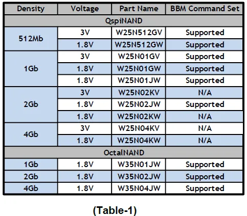
Table 1 Below table shows specific Winbond QspiNAND and OctalNAND that have the block
management command capabilities.
Bad Block Management (BBM) command set
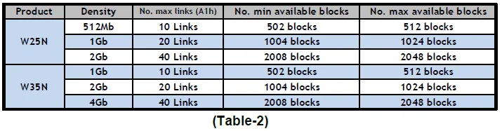
By industry standard NAND flash are allowed to be shipped with certain amount of initial bad blocks found in the factory
testing. The maximum number of bad blocks under typical usage are up to 2% of total number of blocks in the memory
(Table-2). The maximum number of links Bad Block Management command (A1h) can set up is the same as the
maximum number of bad blocks. Based on the application, one may use continuous read. To guarantee a continuous
read operation on the first 1,000 blocks, the manufacturer may have used some of the BBM LUT entrees. It is
advisable for the user to scan all blocks and keep a table of all manufacturer bad blocks prior to first
erase/program operation. Please check with Winbond, as some automotive grade parts may be offered with
zero initial bad blocks from factory
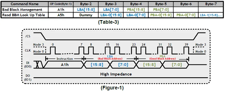
Bad block management command “A1h”(Figure-1) is to set up the link for swapping bad block
(LBA[15:0]) and good block PBA[15:0] (“Block swap”). Before issuing (A1h), the write enable
instruction (06h) must be executed (WEL=1).
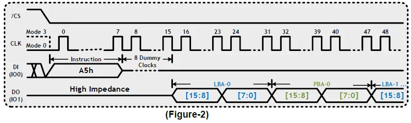
When block swap has been completed, the block swap information will be saved into LUT
(Look Up Table). However, prior to issuing the “A1h”, the user should read the LUT information
by using the command Read BBM Look Up Table “A5h” (Figure-2) to determine which blocks
have been swapped, and as a result, the number of available links remaining. Block addresses
for all links will output sequentially starting 1st link (LBA0 & PBA0) in LUT. If there were available
links that are unused, the output will contain LBA[15:14] as (0,0) data. If there were no available
links, the LUT-F indicator bit (described later) will show that it is full.
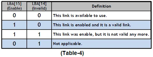
The MSB bits LBA[15:14] of each link are used to indicate the status of the link.(Table-4). Once link
has been set up between bad block(LBA) and good block(PBA), the LBA[15:14]=(1,0). When the
same LBA is registered in multiple Links, the replacement of LBA-PBA is invalid except for the last
registered one, so LBA [15:14] = (1, 1) is outputted for the invalid link. For example, when the same
Block is registered in LBA0 and LBA1 as shown below. In one such scenario, replacement block can
be also bad, and block swap is then repeated, making first link invalid (1, 1) and subsequent link as
valid (1, 0).
LBA0=BLK5, PBA0=BLK1004: This Link is invalid ➔LBA [15:14] = (1, 1)
LBA1=BLK5, PBA1=BLK1005: This Link is valid ➔LBA [15:14] = (1, 0)
The Figure-1 and Figure-2 show the sequence with Single SPI SDR with single die. Please
refer to sequence in each data sheet for the OctalNAND and stacked die products
W25N02JW/W35N04JW.
Bad Block Management Operation
Bad blocks can be found in the factory testing, but can also occur during lifetime usage due
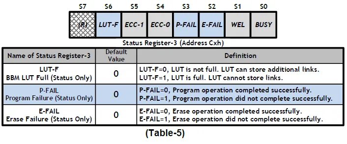
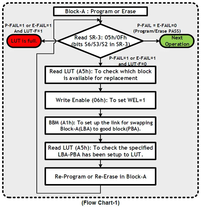
to erase or program failures. It is important to read status register P-Fail and E-Fail bit (Table-5)
in status register-3 after issuing program or erase command to confirm program or erase
operation status. Below flow chart explains the bad block swap flow when there is a program or
erase failure (P-Fail or E-Fail bit =1).
Bad Block Management operation usage case: (QspiNAND 1Gb used as an example)
In order to implement bad block management (bad block swap) into system, it recommends
to reserve the last 2% block area for the bad block swap. This means the user can use block
from block-0 to block-1003 for data storing and reserve block from block-1004 to block-1023 for
bad block replacement.
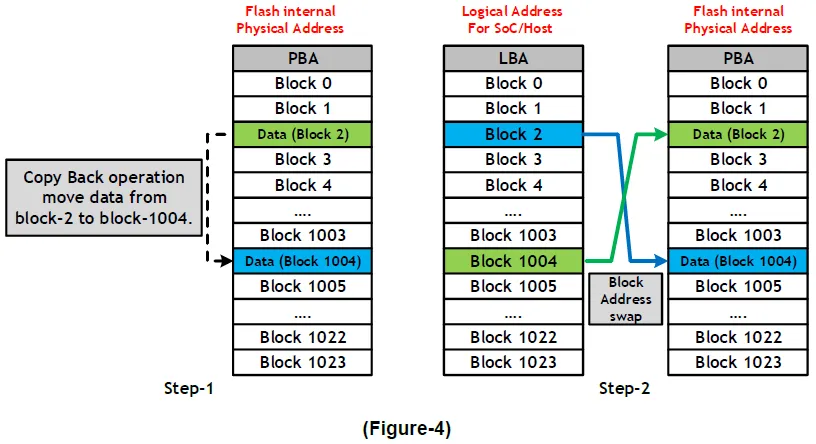
In the Figure-3, if the Block-2 has failed in programming or erasing in NAND 1Gb, the user
can swap bad Block-2 for good Block-1004 by using the command A1h. After block swapping,
the block address will be remapping automatically. The host can access the flash as if it has a
continuous set of blocks with addresses from block-0 to block-1003.
There are two situations where bad block management operation can be combined with copy
back operation. One is when the host knows the block-2 is exceeding P/E cycling limits. The
user can move data from Block-2 to Block-1004 before Block-2 becomes a bad block. Then
using bad block management command (A1h) to swap the block link (Figure-4). Another is when
the host detects program failure, then the user can do block management after copy back. For
more information on the copy back operation,

Please reference Winbond application note “AN0000036 Copy-back operation flow for W25N
QspiNAND and W35N OctalNAND”.
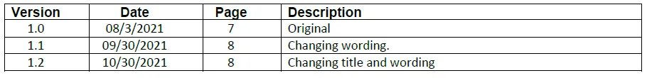
Revision History
Trademarks
Winbond, SpiFlash and SpiStack are trademarks of Winbond Electronics Corporation.
All other marks are the property of their respective owner.
Important Notice
Winbond products are not designed, intended, authorized or warranted for use as components in systems or equipment intended for surgical implantation, atomic energy control instruments, airplane or spaceship instruments, transportation instruments, traffic signal instruments, combustion control instruments, or for other applications intended to support or sustain life. Furthermore, Winbond products are not intended for applications wherein failure of Winbond products could result or lead to a situation wherein personal injury, death or severe property or environmental damage could occur. Winbond customers using or selling these products for use in such applications do so at their own risk and agree to fully indemnify Winbond for any damages resulting from such improper use or sales.
Information in this document is provided solely in connection with Winbond products. Winbond reserves the right to make changes, corrections, modifications or improvements to this document and the products and services described herein at any time, without notice.
AN0000050
Publication Date: Oct 30th , 2021 Revision 1.2
