

Application Note for LPDDR4 Boundary Scan
Table of Contents
1 Preface
2 BALL/ Pad DESCRIPTION
3 Control signals of Boundary Scan
3.1 Single-Channel control signals of Boundary Scan
3.2 Dual-Channel control signals of Boundary Scan
4 Boundary Scan Output Order
4.1 Singlel-Channel sequence of scan data output
4.2 Dual-Channel sequence of scan data output
5 Boundary Scan operation
5.1 Scan Initialization
5.2 Scan Capture Timing
5.3 Scan Shift Timing
5.4 Scan Exit Sequence
6 DC Electrical Characteristics Condition
7 AC Electrical Characteristics Condition
8 Revision History
1 PREFACE
Winbond LPDDR4 device is built with boundary scan chain for users to test the connectivity between memory controller and memory device itself.
The boundary scan chain provide a simply way to check status of connection between memory controller and memory device itself. The boundary scan chain is able to be enabled by a SEN input. All the connection status of each IO between memory controller and memory device will be latched by the scan chain in parallel and be read out from a dedicated output pin serially.
2 BALL/ PAD DESCRIPTION
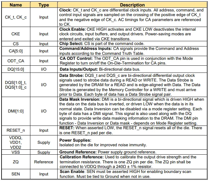
Note: DQSn_t / DQSn_c and ODT_CA pins are excluded from Boundary Scan chain
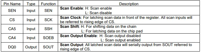
3 CONTROL SIGNALS OF BOUNDARY SCAN
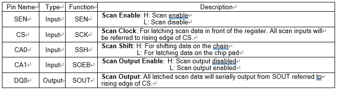
3.1 Single-Channel control signals of Boundary Scan
3.2 Dual-Channel control signals of Boundary Scan
(For channel A)
(For channel B)
4 BOUNDARY SCAN OUTPUT ORDER
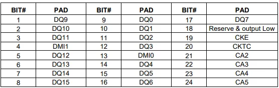
4.1 Single-Channel sequence of scan data output
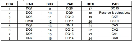
4.2 Dual-Channel sequence of scan data output
(For channel A)
(For channel B)
5 BOUNDARY SCAN OPERATION
When SEN is asserted, no commands are to be executed by the LPDDR4 device. This applies both to user commands and manufacturing commands which may exist while RESET_n is deasserted.
The Scan Function can be used right after bringing up VDD1/VDD2/VDDQ of the device. No initialization sequence of the device is required.
In Scan Mode all terminations for CA and DQ, DMI, DQSn_t and DQSn_c are switched off.
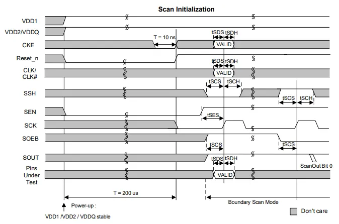
5.1 Scan Initialization
The LPDDR4 device needs to follow the given sequence below to support the boundary scan functionality. There is no external clock for the whole sequence needed.
1. External Voltages (VDD1/VDD2/VDDQ) need to be stable for 200μs, SEN has to be kept low.
2. Bring SEN up to high state to enter boundary scan functionality.
3. Operate boundary scan functionality.
4. Boundary scan can be exited by bringing SEN to LOW or simply by switching power off.
5.2 Scan Capture Timing
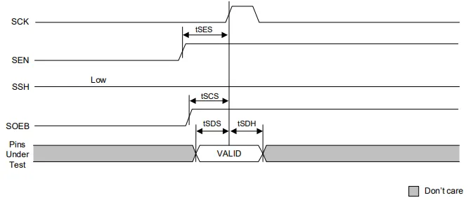
Note:
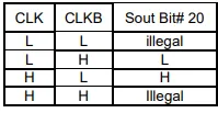
For complementary pins (CLK/CLKB) during BSC test, complementary pin must have different level of input for scan capture. For example, CLK=H / CLKB=L or CLK=L / CLKB=H. Condition of CLK=H / CLKB=H or CLK=L / CLKB=L is not allowed.
5.3 Scan Shift Timing
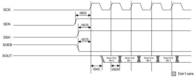
Note:
SCK clock will latch the data in front of each register of the scan chain. The first bit of the scan chain will be output onto the SOUT pin.
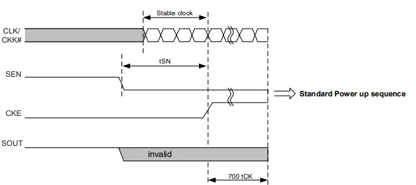
5.4 Scan Exit Sequence
The figure below shows the Scan Exit Sequence. This figure show the exiting of the boundary scan functionality in conjugation with the LPDDR4 initialization sequence to bring the LPDDR4 in a well defined state for normal data access operation. The device will be ready for normal data access operation after standard power up sequence.
6 DC ELECTRICAL CHARACTERISTICS CONDITION
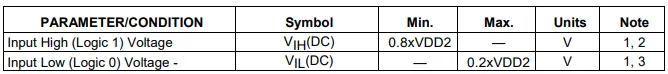
Notes:
1. The parameter applies only when SEN is asserted.
2. VIH voltages referenced to VDD2.
3. VIL voltages referenced to GND.
7 AC ELECTRICAL CHARACTERISTICS CONDITION
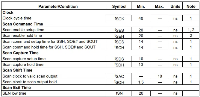
Notes:
1. The parameter applies only when SEN is asserted.
2. Scan Enable should be issued earlier than other Scan Commands by 6 ns.
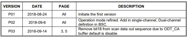
8 REVISION HISTORY