

APPLICATION NOTE
LPDDR2 Precharge/Precharge-All Command to Power-Down Entry

Table of Contents
1. LPDDR2 Device Power Down Function
2. LPDDR2 Device Power Down Entry
2.1 Power Down Entry while Mode Register Read operation in progress
2.2 Power Down Entry while Mode Register Write operation in progress
2.3 Power Down Entry while row activation or refresh in progress
2.4 Power Down Entry while Read operation in progress
2.5 Power Down Entry while Write operation in progress
2.6 Power Down Entry while precharge or auto-precharge in progress
3. Revision History
1. LPDDR2 Device Power Down Function
For LPDDR2 SDRAM, power-down is synchronously entered when CKE is registered LOW
and CS_n HIGH at the rising edge of clock. CKE must be registered HIGH in the previous
clock cycle. A NOP command must be driven in the clock cycle following the power-down
command. Timing diagrams are shown as below with details for entry into power down.
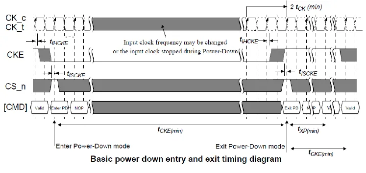
NOTE: Input clock frequency may be changed or the input clock stopped during power-down, provided that
upon exiting power-down, the clock is stable and within specified limits for a minimum of 2 clock cycles prior to
power-down exit and the clock frequency is between the minimum and maximum frequency for the particular
speed grade.
For LPDDR2 SDRAM, if power-down occurs when all banks are idle, this mode is referred
to as idle power-down; if power-down occurs when there is a row active in any bank, this
mode is referred to as active power-down.
Entering power-down deactivates the input and output buffers, excluding CK_t, CK_c, and
CKE. In power-down mode, CKE must be maintained LOW while all other input signals are
“Don’t Care”. CKE LOW must be maintained until tCKE has been satisfied. VREF must be
maintained at a valid level during power down.
VDDQ may be turned off during power down. If VDDQ is turned off, then VREFDQ must
also be turned off. Prior to exiting power down, both VDDQ and VREFDQ must be within
their respective min/max operating ranges.
For LPDDR2 SDRAM, the maximum duration in power-down mode is only limited by the
refresh requirements, as no refresh operations are performed in power-down mode.
The power-down state is exited when CKE is registered HIGH. The controller shall drive
CS_n HIGH in conjunction with CKE HIGH when exiting the power-down state. CKE HIGH
must be maintained until tCKE has been satisfied. A valid, executable command can be
applied with power-down exit latency, tXP after CKE goes HIGH. Power-down exit latency
is defined in the timing parameter table of this standard.
2. LPDDR2 Device Power Down Entry
For LPDDR2 SDRAM, power-down is synchronously entered when CKE is registered LOW
and CS_n HIGH at the rising edge of clock. CKE must be registered HIGH in the previous
clock cycle. CKE is not allowed to go LOW while mode register, read, or write operations
are in progress. CKE is allowed to go LOW while operations such as row activation or
refresh is in progress. CKE also is allowed to go LOW post to a NOP command while
operations such as precharge or auto-precharge is in progress.
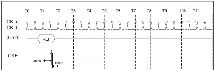
2.1 Power Down Entry while Mode Register Read operation in progress.
For LPDDR2 SDRAM, power-down is synchronously entered when CKE is registered LOW
and CS_n HIGH at the rising edge of clock. CKE must be registered HIGH in the previous
clock cycle. CKE is allowed to go LOW post Mode Register Read operation completed.
Timing diagrams are shown as below with details for entry into power down after Mode
Register Read operation is done.
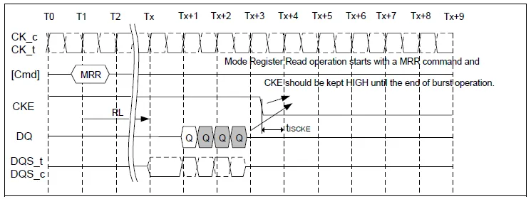
Note: CKE may be registered LOW RL + RU(tDQSCK(MAX)/tCK)+ BL/2 + 1 clock cycles after the clock on
which theMode Register Read command is registered.
2.2 Power Down Entry while Mode Register Write operation in progress.
For LPDDR2 SDRAM, power-down is synchronously entered when CKE is registered LOW
and CS_n HIGH at the rising edge of clock. CKE must be registered HIGH in the previous
clock cycle. CKE is allowed to go LOW post Mode Register Write operation completed.
Timing diagrams are shown as below with details for entry into power down after Mode
Register Write operation is done.
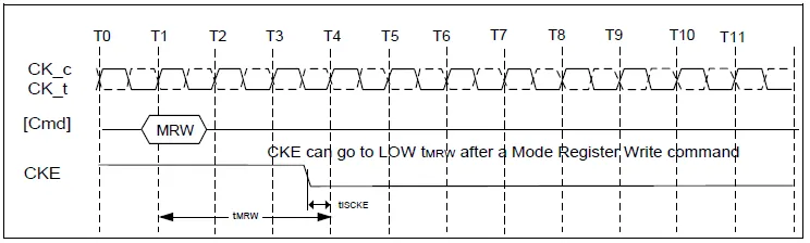
Note: CKE may be registered LOW tMRW after the clock on which the Mode Register Write command is
registered.
2.3 Power Down Entry while row activation or refresh in progress.
For LPDDR2 SDRAM, power-down is synchronously entered when CKE is registered LOW
and CS_n HIGH at the rising edge of clock. CKE must be registered HIGH in the previous
clock cycle. CKE is allowed to go LOW while operations such as row activation or refresh is
in progress. Timing diagrams are shown as below with details for entry into power down
while row activation is in progress.
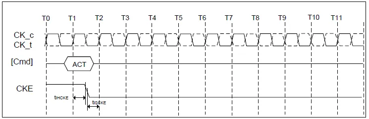
NOTE: CKE may go LOW tIHCKE after the clock on which the Activate command is registered.
Timing diagrams are shown as below with details for entry into power down while refresh is in progress.
Note: CKE may go LOW tIHCKE after the clock on which the Refresh command is registered.
2.4 Power Down Entry while Read operation in progress.
For LPDDR2 SDRAM, power-down is synchronously entered when CKE is registered LOW
and CS_n HIGH at the rising edge of clock. CKE must be registered HIGH in the previous
clock cycle. CKE is allowed to go LOW post read operation completed. Timing diagrams
are shown as below with details for entry into power down after read operation is done.
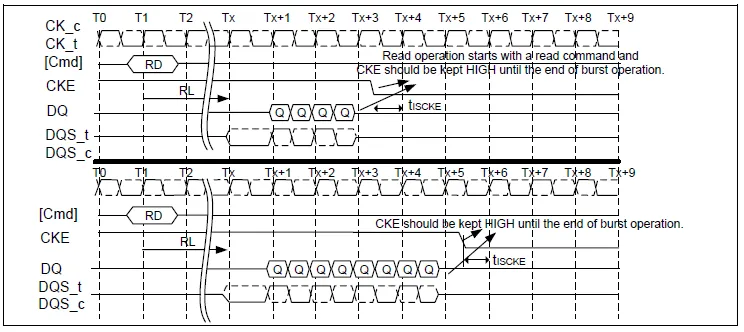
Note: CKE may be registered LOW RL + RU(tDQSCK(MAX)/tCK)+ BL/2 + 1 clock cycles after the clock on
which the Read command is Registered.
2.5 Power Down Entry while Write operation in progress.
For LPDDR2 SDRAM, power-down is synchronously entered when CKE is registered LOW
and CS_n HIGH at the rising edge of clock. CKE must be registered HIGH in the previous
clock cycle. CKE is allowed to go LOW post write operation completed. Timing diagrams
are shown as below with details for entry into power down after write operation is done.
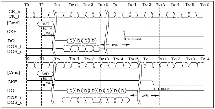
Note: CKE may be registered LOW WL + 1 + BL/2 + RU(tWR/tCK)clock cycles after the clock on which the
Write command is registered.
2.6 Power Down Entry while precharge or auto-precharge in progress.
For LPDDR2 SDRAM, power-down is synchronously entered when CKE is registered LOW
and CS_n HIGH at the rising edge of clock. CKE must be registered HIGH in the previous
clock cycle. CKE also is allowed to go LOW post to a NOP command while operations such
as precharge or auto-precharge is in progress. Timing diagrams are shown as below with
details for entry into power down while precharge or auto-precharge is in progress.
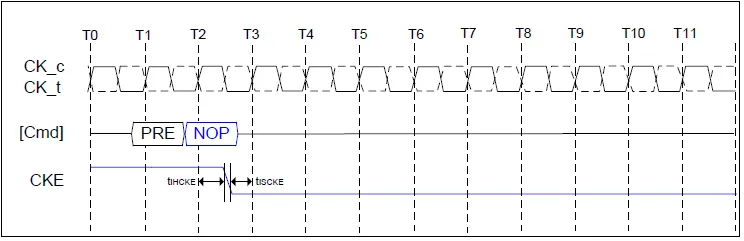
Note: CKE may go LOW tIHCKE after the clock on which the NOP command is registered.
3. Revision History

The above information is the exclusive intellectual property of Winbond Electronics and shall not be disclosed, distributed
or reproduced without permission from Winbond.
Publication Release Date: November 5, 2014
Revision P01-001
