


MIGRATION Guide

Winbond Confidential
MIGRATION Guide W25M02GV TO W25N02KV
2G-BIT 3V
SPI NAND FLASH MEMORY
MIGRATION GUIDE W25M02GV TO W25N02KV
2G-BIT 3V
SPI NAND FLASH MEMORY
Table of Contents
INTRODUCTION
FEATURES COMPARISON
INSTRUCTION SET COMPARISON
AC/DC ELECTRICAL CHARACTERISTICS
PARAMETER PAGE TABLE
DEVICE ID COMPARISON
PART NUMBER COMPARISON
SUMMARY
1. INTRODUCTION
T02KV (2G-bit) NAND Flash memory.
his migration note details how to migrate designs from Winbond W25M02GV (2G-bit) NAND Flash memory to W25N
The W25N02KV (2G-bit) SLC QspiNAND Flash Memory provides a storage solution for systems with limited space, pins and power. The W25N QspiNAND family incorporates the popular SPI interface and the traditional large NAND non-volatile memory space. They are ideal for code shadowing to RAM, executing code directly from Dual/Quad SPI (XIP) and storing voice, text and data. The device operates on a single 2.7V to 3.6V power supply with current consumption as low as 25mA active, 10μA for standby and 1μA for deep power down. All W25N QspiNAND family devices are offered in space-saving packages which were impossible to use in the past for the typical NAND flash memory.
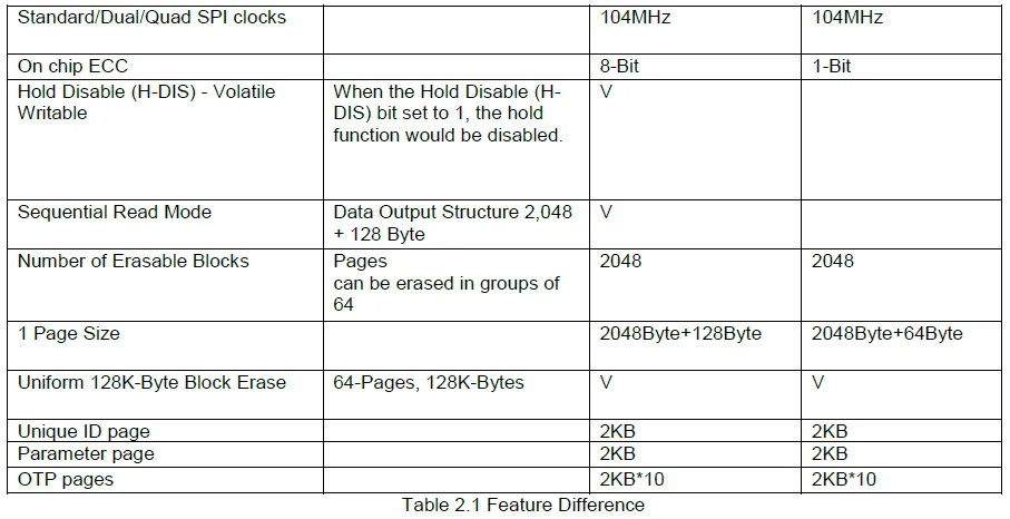
The W25N02KV 2G-bit memory array is organized into 131,072 programmable pages of 2,048-bytes each. The entire page can be programmed at one time using the data from the 2,048-Byte internal buffer. Pages can be erased in groups of 64 (128KB block erase). The W25N02KV has 2,048 erasable blocks.
The W25N02KV supports the standard Serial Peripheral Interface (SPI), Dual/Quad I/O SPI: Serial Clock, Chip Select, Serial Data I/O0 (DI), I/O1 (DO), I/O2 (/WP), and I/O3 (/HOLD). SPI clock frequencies of up to 104MHz are supported allowing equivalent clock rates of 208MHz (104MHz x 2) for Dual I/O and 416MHz (104MHz x 4) for Quad I/O when using the Fast Read Dual/Quad I/O instructions.
The W25N02KV provides a new Sequential Read Mode that allows for efficient access to the entire memory array with a single Read command.
A Hold pin, Write Protect pin and programmable write protection, provide further control flexibility. Additionally, the device supports JEDEC standard manufacturer and device ID, one 2,048-Byte Unique ID page, one 2,048-Byte parameter page and ten 2,048-Byte OTP pages. To provide better NAND flash memory manageability, user configurable internal ECC is also available in W25N02KV.
Note: All the information provided in this guide illustrates only the differences for each section. Please refer to the respective datasheets for more information.
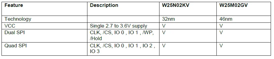
2. FEATURES COMPARISON
Most of the features between W25M02GV and W25N02KV are the same, except a few differences that are highlight in Table 2.1. Refer to the respective W25M02GV and W25N02KV datasheets to verify any other features.
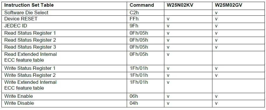
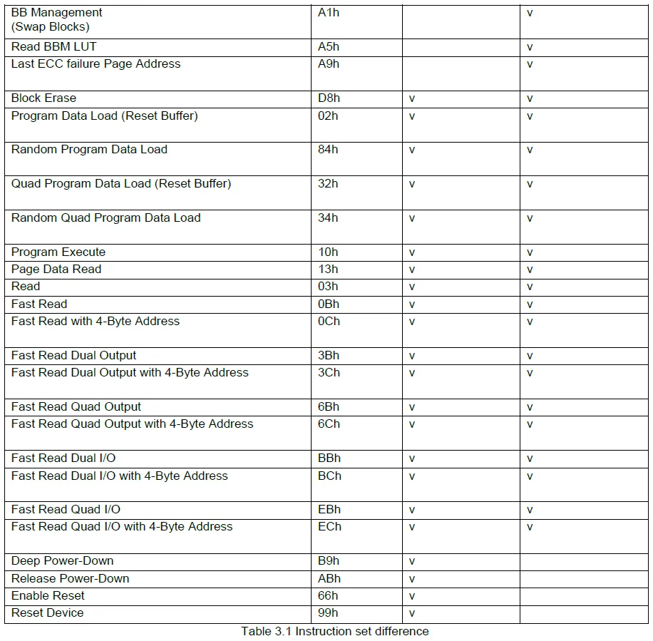
3. INSTRUCTION SET COMPARISON
Most of the instruction set between W25M02GV and W25N02KV are the same, except a few differences that are highlight in Table 3.1.
4. AC/DC ELECTRICAL CHARACTERISTICS
The major AC/DC and differences between W25M02GV and W25N02KV are listed in Table 4.1
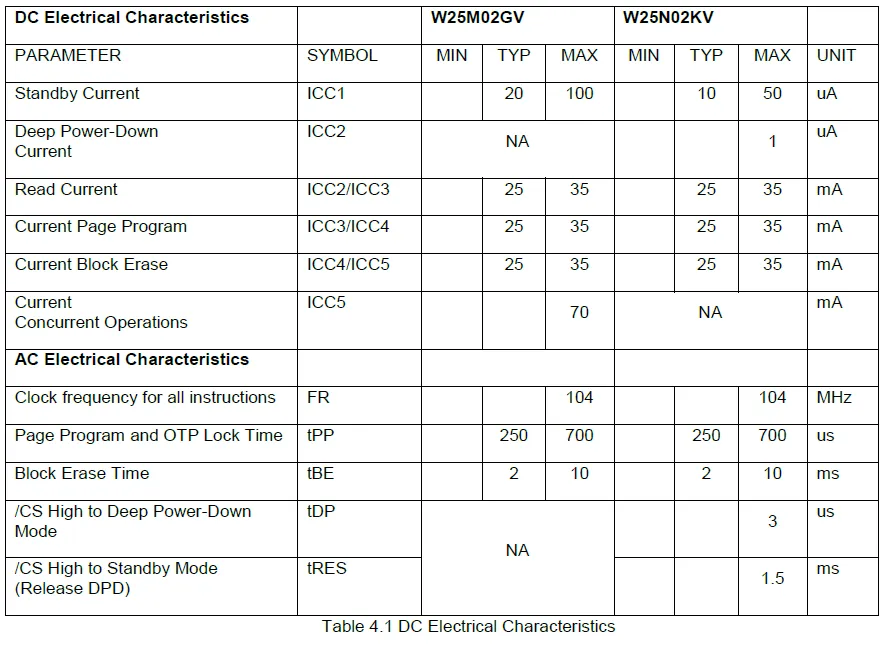
Note:
1. Other AC/DC parameters without list in table3.1 are the same between W25M02GV and W25N02KV. Please refer datasheet for W25M02GV and W25N02KV.
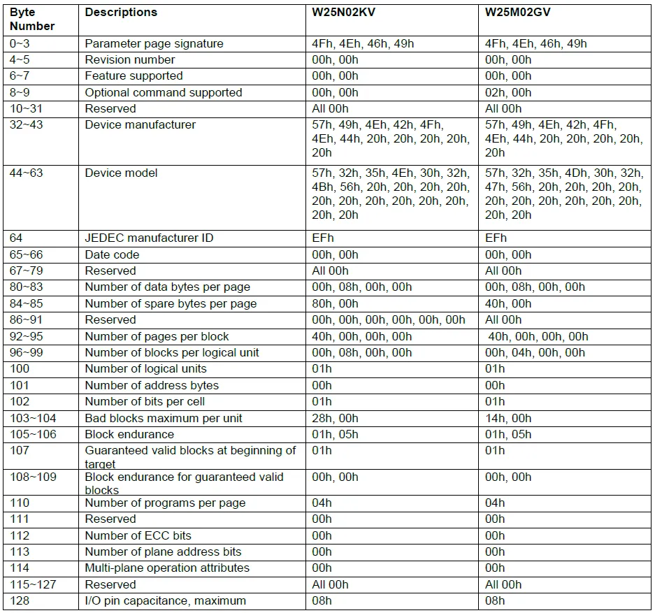
5. PARAMETER PAGE TABLE
The parameter page values of W25M02GV and W25N02KV are listed in Table 5.1
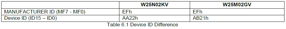
6. DEVICE ID COMPARISON
The device ID differences between W25M02GV and W25N02KV are listed in Table 6.1
7. PART NUMBER COMPARISON
Part number examples for industry temp grade are listed in Table 7.1.
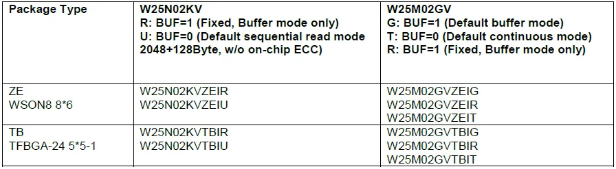
Note. Other temperature grade support please refer to datasheet.
8. SUMMARY
Compared to W25M02GV, the features of W25N02KV are linear address without C2h command, Sequential Read, 2048Byte+128Byte page size and flexible ECC configuration settings. It will need software modification to adopt these differences of features.
For customers transfer from continuous read mode parts W25M02GVxxIT to sequential read mode part W25N02KVxxIU, it will need software ECC or SoC hardware ECC support.
Revision History

Trademarks
Winbond, SpiFlash and SpiStack are trademarks of Winbond Electronics Corporation.
All other marks are the property of their respective owner.
Important Notice
Winbond products are not designed, intended, authorized or warranted for use as components in systems or equipment intended for surgical implantation, atomic energy control instruments, airplane or spaceship instruments, transportation instruments, traffic signal instruments, combustion control instruments, or for other applications intended to support or sustain life. Furthermore, Winbond products are not intended for applications wherein failure of Winbond products could result or lead to a situation wherein personal injury, death or severe property or environmental damage could occur. Winbond customers using or selling these products for use in such applications do so at their own risk and agree to fully indemnify Winbond for any damages resulting from such improper use or sales.
Information in this document is provided solely in connection with Winbond products. Winbond reserves the right to make changes, corrections, modifications or improvements to this document and the products and services described herein at any time, without notice.
Publication Date: Aug 30, 2021 Revision
