


Migration Guide from W29N02GV to W29N02KV
Introduction
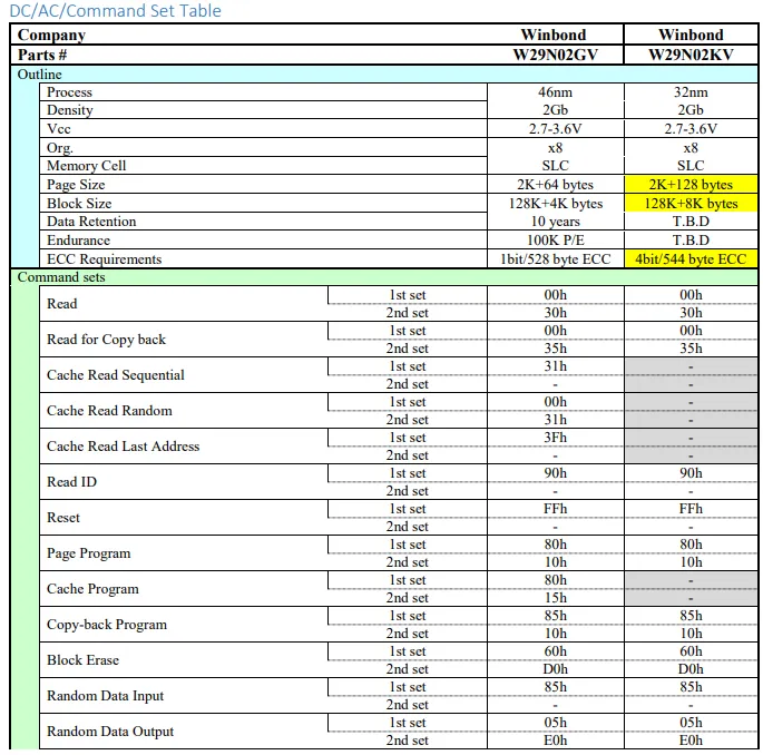
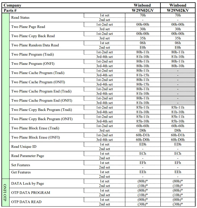
This application note details how to migrate designs from Winbond W29N02GV (2G-bit) NAND Flash memory to W29N02KV (2G-bit) NAND Flash memory.
The memory array of W29N02KV totals 285,212,672 bytes, and organized into 2,048 erasable blocks of 139,264 bytes. Each block consists of 64 programmable pages of 2,176-bytes each. Each page consists of 2,048-bytes for the main data storage area and 128-bytes for the spare data area (The spare area is typically used for error management functions).
The W29N02KV supports the standard NAND flash memory interface using the multiplexed 8-bit bus to transfer data, addresses, and command instructions. The five control signals, CLE, ALE, #CE, #RE and #WE handle the bus interface protocol. Also, the device has two other signal pins, the #WP (Write Protect) and the RY/#BY (Ready/Busy) for monitoring the device status.
Note: All the information provided in this guide illustrates only the differences for each section. Please refer to the respective data sheets for more information.
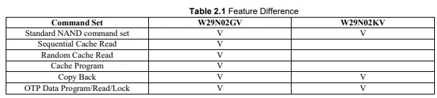
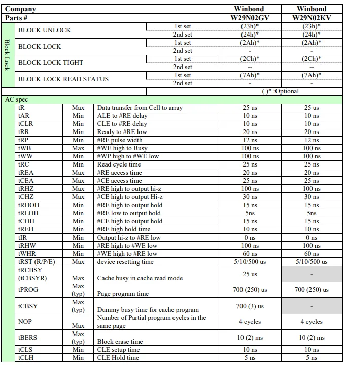
Features Comparison
Most of the features between W29N02GV and W29N02KV are the same, except a few differences that are highlight in Table 2.1. Refer to the respective W29N02GV and W29N02KV data sheets to verify any other features.
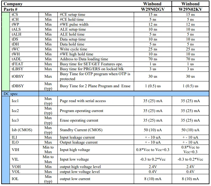
DC Electrical Characteristics
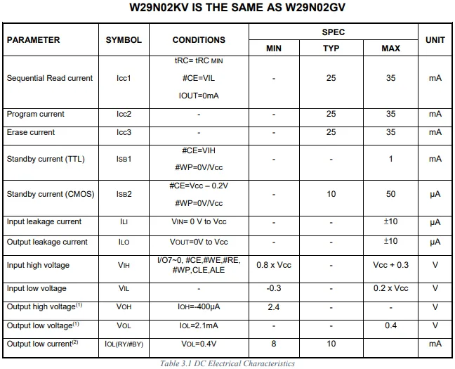
Note:
1. VOH and VOL may need to be relaxed if I/O drive strength is not set to full.
2. IOL (RY/#BY) may need to be relaxed if RY/#BY pull-down strength is not set to full
AC timing characteristics for Operation
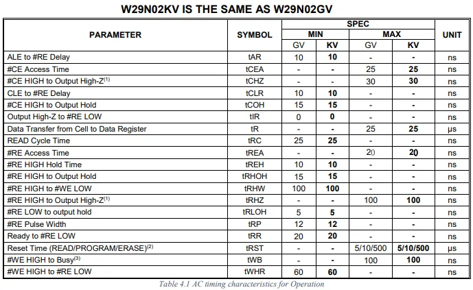
Notes:
1. Transition is measured ±200mV from steady-state voltage with load. This parameter is sampled and not 100 % tested.
2. The RESET (FFh) command is issued while the device is idle, the device goes busy for a maximum of 5us.
3. Do not issue new command during tWB, even if RY/#BY is ready.
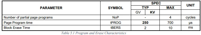
Program and Erase Characteristics
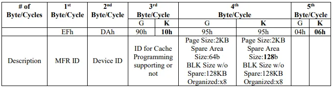
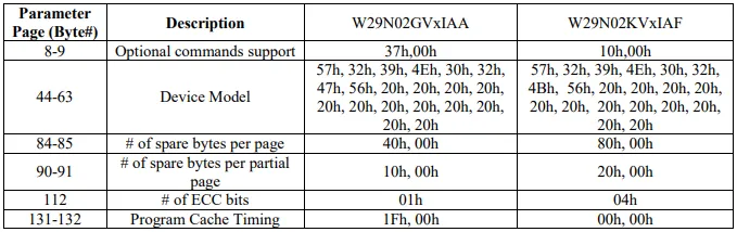
Device ID
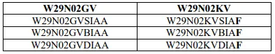
Part number comparison
Summary
The difference between W29N02GV (2G-bit) NAND Flash memory and W29N02KV (2G-bit) NAND Flash memory is the features innovation, its respective device ID and the ECC coding requirement. All other standard ONFI command set are the same with each other. Customers can easily migrate from W29N02GV to W29N02KV.
Comparison Table
Parameter Page Table
Revision History

Trademarks
Winbond, SpiFlash and SpiStack are trademarks of Winbond Electronics Corporation.
All other marks are the property of their respective owner.
Important Notice
Winbond products are not designed, intended, authorized or warranted for use as components in systems or equipment intended for surgical implantation, atomic energy control instruments, airplane or spaceship instruments, transportation instruments, traffic signal instruments, combustion control instruments, or for other applications intended to support or sustain life. Furthermore, Winbond products are not intended for applications wherein failure of Winbond products could result or lead to a situation wherein personal injury, death or severe property or environmental damage could occur. Winbond customers using or selling these products for use in such applications do so at their own risk and agree to fully indemnify Winbond for any damages resulting from such improper use or sales.
Information in this document is provided solely in connection with Winbond products. Winbond reserves the right to make changes, corrections, modifications or improvements to this document and the products and services described herein at any time, without notice.
AN0000025
Publication Date: January 22, 2019 Revision 1.0
